Taiwan's LED Lighting Industry Gets Brighter With Smart Technologies
Dr. J.D. Huang unveils metal-b
2010/06/02 | By Ken LiuTaiwan's light emitting diode (LED) industry has developed many appreciable technologies to offset its shortage of patents on key LED technologies as white-LED ingredient and phosphor formula.
Taiwan leads the global LED supply by volume but far lags Japan in value, suggesting Taiwan's production of low-end LEDs. So developing patented technologies will undoubtedly help make up for such difference. Many LED technologies introduced by local organizations involve packaging and AC chip.
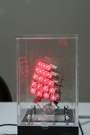
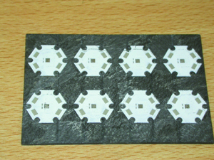
One such technology is “cubic packaging methodology” invented by a team led by Dr. Chien-jen Sun, deputy director of Optoelectronics Device and System Application Division of Electronics & Optoelectronics Research Laboratories (EOL) under the government-backed Industrial Technology Research Institute (ITRI).
Enlarging Surface Area
Based on an age-old scientific theory of area being correlated with reactions involving that area, Sun says, “CPM increases surface area of packaged LEDs by creating extra surfaces, hence enhancing heat dissipation from the core. In contrast, most packagers use flat packaging.”
“Another advantage of CPM is its fewer resistive interface layers. We employ unique technology to eliminate packaging for circuits, substrates, and wires inside the packaging to reduce the number of layers, which is how we keep heat resistance inside a 3-cubic-centimeter packaging to under 0.3C-per-watt.” This is a patented technology.
“For a long time, cooling was a major issue causing midstream and downstream manufacturers to mutually point fingers for defective technology, which we hope to overcome with CPM,” says Sun.
The 3-cubic-centimeter package is designed to facilitate modular building of lighting by simple snap-together assembly.
Although Taiwanese LED makers have been able to cut diode prices since having begun mass production in 2000, Sun says, “Breaking into the lighting market has been impossible due to the excessive heat issue.”
Therefore Forward Electronics is using CPM to develop 10W lighting modules that work as general lighting, automotive lighting, and billboard lighting.
The CPM is a sub project of the laboratories' “Houyi Plan,” named after a mythical hero who shot down nine of the 10 suns scorching China in ancient times. “We believe that LEDs will replace most light sources just like Houyi brought down those nine suns,” says Dr. Chan Yijen, EOL's general director, trying to rationalize the witty project name.
The Houyi plan will help Taiwan's LED-lighting manufacturers to continue growing in the market, with the program focusing on ultra-bright white LED technology and encompass wafer, chip, packaging, and application systems.
With the ultimate goal to give off maximum lumen per dollar, Chan says that the program aims to build white-light LED lamps rated at 100-120 lumen-per-watt but at US$5 per 1,000 lumens, a threshold that allows commercial competitiveness.
Super-conductive Substrate
One more scientist whose achievement deserves citation is Dr. Jen-dong Huang, manger of the Division of Metallic Materials Research at the Materials & Device Thermal Management Laboratory under the ITRI, who recently unveiled metal-based composite packaging substrates rated at 200~800 W/M Kelvin.
Huang notes LEDs turn only 15-20% of electricity into light and the rest as heat, which has to be effectively ventilated to prolong LED durability that would otherwise compromises luminosity.
Cooling a Hurdle
Cooling remains a hurdle for packagers despite high-powered, super-bright LEDs becoming more popular. The race to build brighter LEDs, says Huang, is pushing more packagers to adopt multi-chip and chip-on-board packaging solutions that call for building more efficient cooling solutions. “Choosing packaging substrates calls into consideration of not only thermal-conductivity efficiency of materials but also compatibility of CTE or coefficient of thermal expansion with LED chips. Makers have to minimize heat stress and deflection of substrates due to heat circulation to maximize LED packaging durability.”
Sun spent about six years to develop the substrate program before discovering the metal-based composite formula, noting that metal-based composites have relatively higher thermal conductivity and low CTE, or undergo less expansion due to heat, merits of which are drawing material specialists worldwide to also develop their own formula. Better cooling characteristics mean better LED packaging, says Huang.
Huang's composite material formula is a proprietary secret, consisting of diamond powder, carbon fiber, graphite, and silicon carbide mixed with aluminum or copper powder. Repeated tests at the ITRI lab show Huang's advanced material display outstanding properties, some of which even exceeding those developed by global counterparts.
Huang's formula effectively limits CTE under 8ppm/K and density under 2.5 grams/ml while conducting heat at an excellent 200~800W/m.K. “Effective thermal conductivity means lesser thermal resistance to facilitate thermal transmission to minimize hot spots on LEDs. Packaging reliability and lifespan is a function of the compatibility between LED device and packaging substrates in terms of CTE, or in simpler terms the former two performances vary according to how well LED device and packaging substrates are designed to work together based on CTE. When such criteria are met, LED devices can be directly attached to substrates to further improve cooling,” Huang elaborates.
The metal-based substrates, while more effective in cooling, is also electrically conductive, so a surface-mounted dielectric layer is needed as insulation to prevent shorting, with such insulation being usually a polymer.
More Cost-effective
Unlike metal-core substrates, Huang's composites boast high CTE compatibility, making them suitable for larger LED packaging for maximum size can be as big as 12”-square. Also cost effective, Huang's composites are priced only half as much as equivalents supplied by manufacturers overseas and yet feature certain superior properties. “The composites are quite reliable, and the next step is to improve their capacity for integration with LED systems as modules and housings,” he says, adding such composites have been patented twice in Taiwan and are patent pending in the U.S.
Dr. James Chu's AC LED and LED healthcare lighting are both patented and will help Taiwan sharpen its competitiveness in the LED industry by generating royalty income. The director of EOL's Opto-Electronics Device and System Application Division (ODSAD) leads the two projects.
Semiconductor devices, as computer chips and LEDs, are designed to work inherently at low current, hence needing DC transformers to work off 120V household current.
However, transformers, as other electrical devices, also have resistance and hence impede around 30% of current, compromising electro-efficiency. So ideally a designer wants to raise LED's current tolerance to do without transformer so LEDs can work directly off household current, Chu says
The ODSAD came up with etching “micro-LED circuits” on LED chips, which are then connected in series via “bridge” circuits. “A single LED chip can only accept low voltage, but a series-connected LED circuits on one chip can handle high voltage. So the obvious solution is to etch more such devices on one chip to raise voltage, Chu says.
The “bridge” carries AC current between anodes and cathodes. “Before raising the voltage capacity to household levels, the negative-to-positive current would damage LEDs, but installing rectifiers can redirect currents the other way. Raising current capacity and removing DC transformer enables working with AC, Chu continues.
Changing DC to AC makes LEDs more energy-efficient. In addition, the technology simplifies LED lighting design to cut costs by eliminating transformers that add to cost, he notes.
Why Not AC to Start?
So one is justified to ask why did LED originators not build AC LED lights? “First and foremost, low-voltage technology is mature and cost efficient. Furthermore, powering low-voltage chip with 120V household current is very complicated, the director stresses. “Micro devices are not etched on DC chips, but just the reverse on AC chips. Naturally yield rates on micro devices are much harder to control than DC chips,” he says. His organization is reportedly the world's first to overcome such complexity building computer chips on LED chips.
“For a long time, manufacturers have stayed away from AC for its prohibitive development costs due to technological complexity. But our breakthroughs have literally lit the light at the end of the tunnel for AC LED proponents,” he explains. So far, ITRI's AC LED technology has won at least 70 patents covering structure, chip, packaging and application, as well as the R&D 100 Awards from the renowned R&D Magazine of the U.S., founded in 1963 to honor, recognize innovative products yearly with its “The Oscars of Invention.”
The ODSAD has developed AC chips rated from 1~5W in output. “We have achieved 50 lumens-per-watt with the chips, enabling a five-watt emitter to produce 250 lumens. You'd need 30-45W incandescent bulbs to equal such brightness,” Chu says. The organization aims to boost the performance to 80 lumen-watt after 2010.
Chu says field tests show the AC LEDs becoming brighter after 2,000 hours of nonstop operation, suggesting need for further studies to identify such irregularity. But AC LED has excellent lifespan compared with DC LED, Chou stresses.
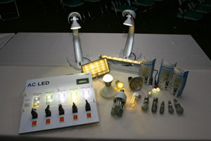
To show practicality, the ODSAD has built a desk lamp with AC LEDs. Plus four enterprises in Taiwan have been licensed to make the LEDs, including chipmaker Epistar Inc. and consumer-electronics manufacturer Forward Electronics Co., Ltd., a Tatung Group affiliate that is ready to mass-produce AC LEDs.
AC appliances are considered hazardous for carrying high voltages, so Chu's organization has co-developed safety standards for AC LEDs with UL Taiwan to address such issue in Taiwan.
Strategic Alliance
To help Taiwan's LED industry quickly apply AC LEDs, the ITRI has helped organize over 20 local manufacturers, including Epistar, Lite-On Technology Corp., Forward and Tyntek Corp., to form a strategic alliance. Johnsee Lee, ITRI president, pointed out at the inauguration that forming such alliance would “help Taiwan's LED industry move up the value chain to create high-value products and advantages.”
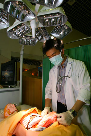
ODSAD's triple-patented LED healthcare lighting technology is almost as brilliant as its AC LED, meeting the need in healthcare settings of good color rendering, low shadow, low temperature and luminosity, making it ideal for surgery, according to Chu.
This 9,000 lumen light, with 45% to 60% less shadow at one meter, makes ideal operating room lighting for better visibility for surgeons. Also, such light is cooler with less infra-red wavelengths being emitted, offering more comfort and improved visual definition to surgeons, especially during prolonged operations.
Chu figures the leading-edge healthcare LED lighting technology to help LED manufacturers in Taiwan to tap special-purpose lighting segments, or around 20% of the US$90 billion lighting market.
Unorthodox Packaging Methodology
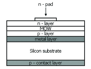
High Power Opto Inc. Chief Executive K.H. Huang, a Northwestern University Ph.D in materials science and veteran of Taiwan's LED industry, has made claim to fame via unorthodox packaging methodology—fixing the III-V semiconductor layers such as GaN (gallium nitride) on silicon wafer.
Traditionally, epi-wafer makers grow the layers on sapphire disks and then slice them into chips for packaging. “But the point is that sapphire is a poor heat conductor at 35-40W/mK, compared with silicon's 125 to 150W/mK, in spite of its good light transmittance. Furthermore, significant improvement in LED illumination has suggested sapphire's weakness,” Huang analyzes.
Huang stresses that thermal dissipation solutions for high-power LEDs should not simply address system, module and package. “In fact, the dissipation on chip is the most important of all as the illumination substances are deposited on the surface of chip. They are much more susceptible to heat than the circuits on the chips. So when the layers are destroyed by heat, dissipation efforts for other devices would be only in vain,” he analyzes.
Limited in Capacity
Huang concedes silicon has its ceiling limit, making it suitable for LED light bulbs rated at 1W~3W, based on its properties. Copper substrate is recognized to have the best heat conductivity at 300 to 400W/mK, ideal for higher-power LED bulbs. “But silicon is more cost efficient than copper in terms of economy-of-scale of silicon wafers than copper substrates, driven by the robust chip making industry,” he explains.
High Power Opto has put silicon-substrate LED wafer into mass production, becoming another epi-wafer manufacturer using silicon technology after Cree of the United States and Osram of Germany. “But our technology is not the same as theirs and we have our exclusive patents,” Huang stresses. Huang says his company has applied for at last 10 patents on the silicon technology.
Patented Layer-removal
The company's patents are mainly awarded for the methodology of removing semiconductor layers from sapphire. “We use an evaporation technology to neatly remove the layers from sapphire, neither damaging the layers nor the sapphire,” he says. The layers are mounted and affixed on a silicon wafer with eutectic die attachment approach mixing gold with iridium at 250 Centigrade degree. The alloy constitutes a good light conductivity mechanism to make up for the disadvantage of silicon in this performance.
High Power Opto now is able to produce si-based LED chip dies at size bigger than 40x48 square mil (around 1.01x 1.21 square millimeter). “The primary advantages of our technology are the high illumination output from front side of the chip, low light from side and back ends, and one single wavelength of light that generates consistent color bin,” Huang stresses.
The company, according to Huang, is using the technology to produce red, yellow and green chips, which have been assembled into affiliate Excellent Opto Inc.'s packages and lighting fixtures. “We're now depending on red and yellow chips for revenue of US$1.5 million a month,” he says.
Now, the company has boosted output of si-based red and yellow chips to 200 million units combined a month from 2009's 120 million chips. The company is said to have snatched up over half of the world's market of high-power red, yellow LED chips.
To keep up with market uptrend, High Power Opto is constructing a new two-hectare factory at the Central Taiwan Science Park, which will at its completion double the company's output of red and yellow chips combined and boost its revenue to US$156 million) a year initially with its 25 metal organic chemical vapor deposition (MOCVD) chambers. In the meantime, the company has started developing si-based blue chips and will produce the chips at the new factory to offer customers maximum chromaticity range of chips.
